


Aesthetics|High efficiency|High reliability|High power output per watt
Features
- Full area illuminated
- All c-Si atoms electricity-producible technology
- All back electrode technology
- All back passivating contact technology
- Totally Ag-free metallization technology
- Whole Life-cycle hot-spot risk control and Power generation guarantee technology
Description
Tackling N-type technical barriers, fully independent propertyrights
Relying on the first star product developed by Lianchuang Center, AIKO self-developed core equipment and mass production process, which has completely independent intellectual property rights.
Silver-free metallization historic technological breakthrough
ABC silver-free technology guarantees power generation, while it can greatly reduce the problem of broken grid of crystalline silicon cells, it can also avoid affecting the life of components due to the life of silver wires.
Revolutionary N-type full back contact battery product
There is no metal grid on the front, 100% sunlight is received, and it has excellent light decay resistance performance and mechanical load performance; Low temperature coefficient, higher temperature resistance, high efficiency and high appearance.
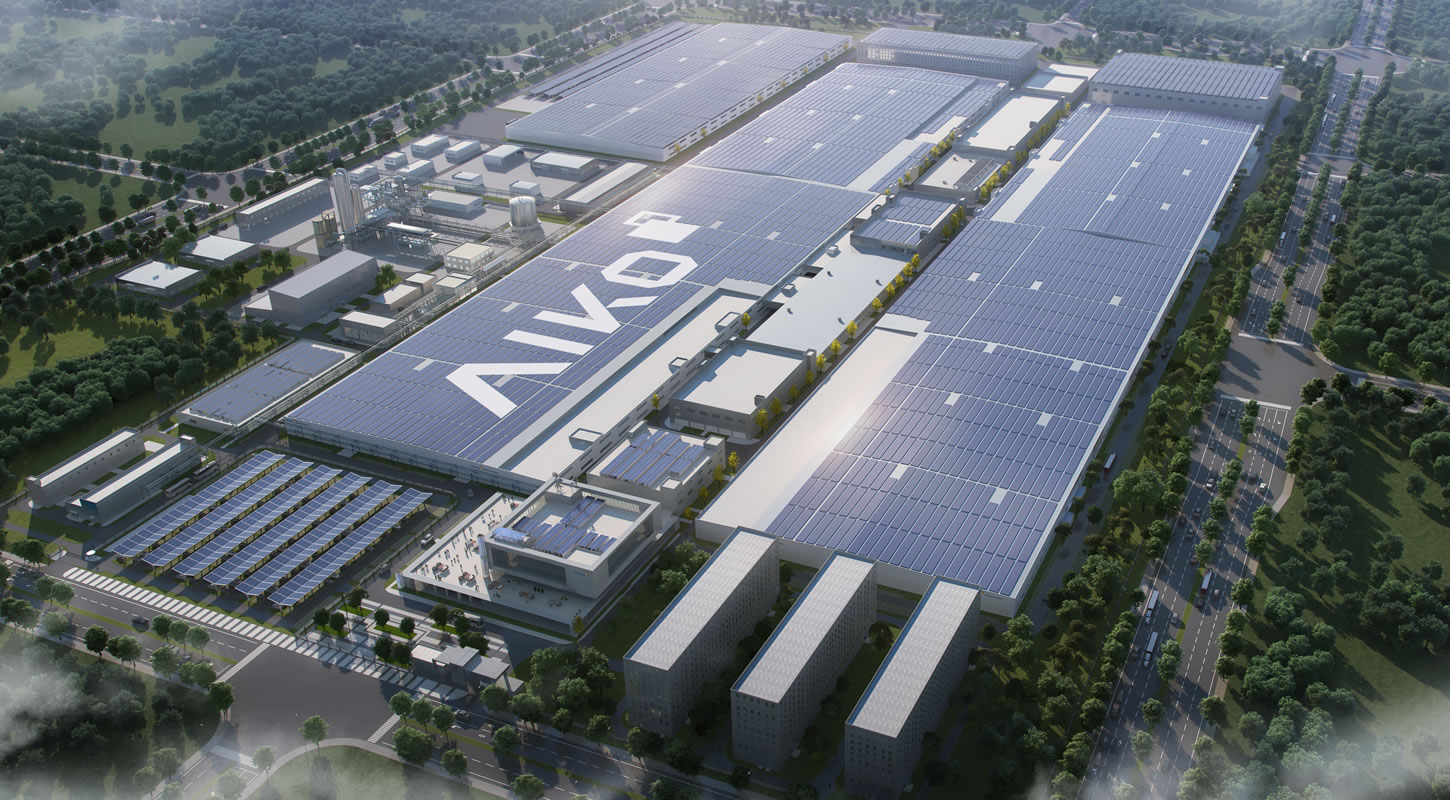
New intelligent manufacturing factory in Zhuhai
In Q4 of 2022, 6.5GW will be put into operation in AIKO Zhuhai Base, the Zhuhai base covers an area of ??about 1,100 mu, with a designed production capacity of 26GW. In Q3 of 2023, 10GW of ABC cell and module production capacity will be formed.
Broad prospects for technological development
In the future, ABC can be combined with perovskite, copper indium gallium selenide, cadmium Telluride, thin-film solar cells and other technologies superimposed.
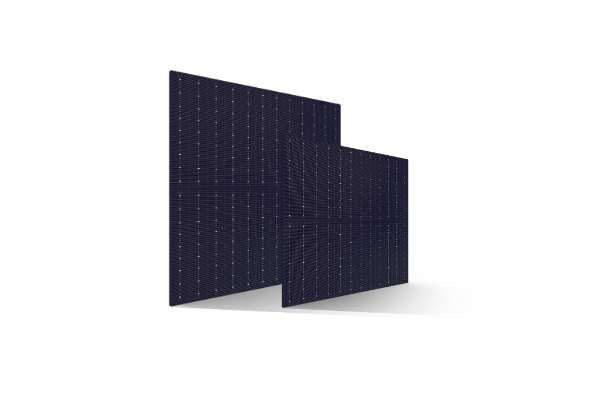
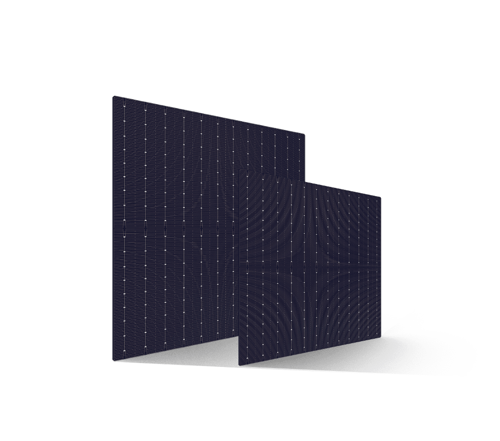
High efficiency|High reliability|High power yield|“Bifacial, metrology, and classification” technology
Size
- 182mm×182mm(diameter 247±0.5mm)
- 210mm×210mm(diameter 295±0.25mm)
- Thickness:160±20μm
Features
182mm 10BB Bifacial Mono PERC Cell
- Front Side (?): Silicon oxide + blue silicon nitride compound anti-reflection coating (PID Free) ; The front side is a half-cut design; The busbar head is a large double fork, and the pads of the busbar are intermittently stepped. The size of the head pad is 1.2 ± 0.15mm * 1.3± 0.15mm, and the middle pad of the busbar size is 0.8±0.15mm*1 ± 0.15mm.
- Back Side (+): Passivated layer (AlOx and SiNx) and Rear Contact (Al); the rear electrode is composed of 10 roots rear compound busbar and 160 roots rear Al fingers. The composite busbar is locally narrowed, and the width is 1.5 ± 0.3mm and 1.0 ± 0.3mm, respectively. 8 sections 1.45±0.3 mm silver anode, no laser pattern under the rear electrode. Silver electrode has round head, and silver electrode is 1.5±0.6mm hollow at both ends.
210mm 12BB Bifacial Mono PERC Cell
- Front(-):Silicon dioxide + blue nitride composite anti-reflection film (PID free);Three-Segment design,12 roots bus bar and 120-180 roots fingers;The bus bar width is 0.06±0.02mm with three-Segment design, and the bus bar has two forks head (size (1.3±0.2)mm × (1.0±0.1) mm) ;the size of 4 padsat the junction of bus bar and the fingers is (1.2±0.2)mm × (0.5±0.2)mm.
- Back(+):AlOX and SiNX dual layer and rear contact; the rear electrode is composed of 12 roots rear compound bus bar and 150-250 roots rear Al fingers,8 sections,1.4±0.3 mm silver anode.
210mm 9BB Bifacial Mono PERC Cell
- Front(-): Silicon dioxide + blue nitride composite anti-reflection film (PID free);Three-Segment design,9 roots bus bar and 120-180 roots fingers; The bus bar width is 0.08±0.03mm with three-Segment design, and the bus bar has two forks head (size (1.5±0.1)mm × (1.2±0.1) mm) ; the size of 4 padsat the junction of bus bar and the fingers is (1.5±0.15)mm × (1.0±0.15)mm.
- Back(+):AlOX and SiNX dual layer rear contact; the rear electrode is composed of 9 roots rear compound bus bar and 150-250 roots rear Al fingers,9 sections,1.8±0.2 mm silver anode.

for a Bespoke
Energy System